
Fabricating My Own Integrated Circuits


This class was a really great opportunity to get hands-on experience in a clean room and fabricate CMOS circuitry using a basic CMOS manufacturing procedures. Besides, not everyone gets a chance to make their own wafers from scratch!
In the lab we were able to:
-
Perform common fabrication processes used in microelectronics fabrication.
-
Test integrated circuits and interpret non-ideal behaviors.
-
Correlate non-ideal IC behavior back to the processes used to fabricate the device under test.
-
Model IC physical parameters such as junction depth, dopant concentration and modify fabrication process flow designs to improve device performance
-
Write technical reports related to the laboratory experiences, integrated circuit characterization, and a process design project.
-
Compile a Process Design Project including analyzing non-ideal performance of fabricated ICs, developing a process flow to improve performance
The course covered all of the topics needed for a solid understanding of the integrated circuit fabrication process by covering topics such as:
-
Semiconductor Materials
-
Crystallography
-
Oxidation
-
Photolithography
-
Diffusion
-
Wet/Dry Etching Tech
-
Plasma Processing
-
Metallization
-
Ion Implantation
-
CVD Processes
-
MEMS Processes Integration
This was part of a class where we fabricated and tested the ICs that we made in lab.
Now more about the chips!
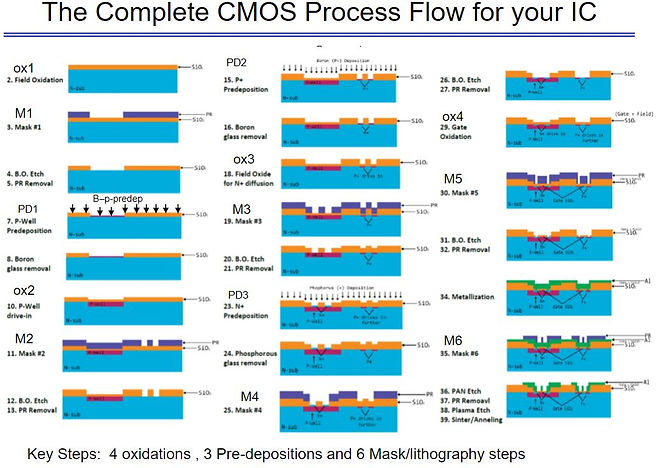
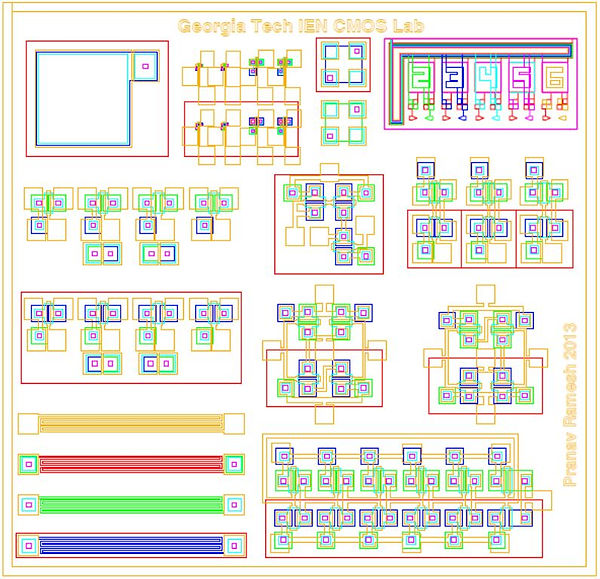
The wafer has 42 functional chips on it. Each chip has a number of components. To create the components, the wafer must go through 39 different steps during the fabrications process. These processes are mostly a series of making a chemical 'mask' and then exposing parts of it to UV light to change the chemical properties and then using another chemical to remove the exposed areas.
But what about what's on the chips?
Each chip has 7 unique devices on it. There are more than 7 total devices because some are made with different line widths or lengths. The devices on the chip are resistors (bottom left), a ring oscillator (bottom right), nand and nor gates (above the ring oscillator), mosfets with attached diodes (above the resistors), a capacitor (top left), and inverters (above the nand nor gates). You can read more about each component by clicking on them below!
You'll also notice the numbers and shapes across the tops. That's what is used to ensure proper alignment during the exposure steps.


